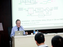
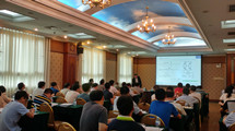
What we provide? 我们为您提供全方位的集成电路人才培训与学习解决方案
林恩咨询以“客户的成功,我们的成功”为价值导向,我们积极配合国家集成电路相关产业政策,打造专业集成电路人才培训与学习服务平台,我们为企业、非盈利组织和公共机构、个人提供全面的培训解决方案和咨询服务,包括集成电路、微电子产品、物联网等专业人才培训、技术交流、技术咨询......
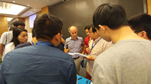
定制个性化课程
无论您所处产品设计、芯片制造、封装测试还是设备材料、智能卡……
我们都会针对您所处集成电路产业链中不同的培训需求及自身存在的问题,为您定制个性化的培训课程!

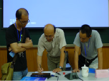
选择适合您的培训方式
世界正成为一个平台,您的团队也必须与世界同步,电话、视频、网络会议、电子邮件……
出差频繁、雇员水平参差不齐……
我们的Blending- Learning策略将为您提供最佳解决方案,实现培训、管理的无缝整合!
Why us? “术业有专攻”——专业的人做专业的事,才能实现资源的最优配置!

作为专业的企业培训公司,林恩咨询致力于为企业提供合理建议和最优方案!帮助我们的客户应对挑战,取得成功……
Value-added services! 我们一直致力于为客户提供最有价值的服务

- 免费方案:设计培训方案,书写培训报告;
- 免费评估:对培训效果进行评估;
- 免费测评工具:对雇员进行评估,帮助企业选人、用人;
- 免费短信、邮件信使服务;
- 免费全程培训管理;
- 提供个性化培训解决方案;
- 领先业界On-line Course在线课程;
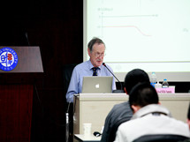
参加过培训客户 Our Clients
 是德科技(中国)有限公司
 中国科学院上海微系统所
 中国电子集团公司
 艾迪悌科技(上海)有限公司
 中芯国际
中芯国际 亚诺德半导体
 深圳市海思半导体
新闻动态 Our News
案例展示 Our Case